June Power June Power

Top Ways to Minimize Energy Loss During Power Conversion

Time:2026-09-08 Author:Mason
0%

Every power converter wastes some energy as heat, noise, magnetic loss, or switching stress. The goal is not perfection. It is controlled, measurable improvement.

This guide explains practical ways to Minimize Energy Loss During Power Conversion across industrial, commercial, and embedded systems. Engineers can begin with accurate load profiles, efficiency measurements, and reliable component datasheets. A converter operating near its ideal load may perform differently at startup, standby, or sudden demand changes. Small details matter. A warm inductor matters.

Selecting efficient switching devices is important, but device choice alone cannot solve every problem. Proper gate-drive timing, suitable switching frequency, and low-resistance connections can reduce unnecessary losses. Thermal imaging can reveal hot terminals, crowded circuit paths, and cooling weaknesses. An oscilloscope may expose voltage spikes that ordinary efficiency tests miss. These tools support decisions based on evidence rather than assumptions.

Layout also deserves careful attention. Short current loops can reduce parasitic resistance and electromagnetic stress. Adequate airflow, heat sinking, and operating temperature control can protect long-term performance. However, every design involves trade-offs. A higher switching frequency may shrink magnetic components while increasing switching losses. A cheaper capacitor may pass initial testing yet age faster under ripple current. Measurements can still be imperfect, especially when sensors, cables, or test conditions add error. Reliable results require repeatable methods, calibrated equipment, and realistic operating scenarios. This article focuses on those practical choices, while acknowledging that the best solution depends on the converter topology, power range, environment, and expected service life.
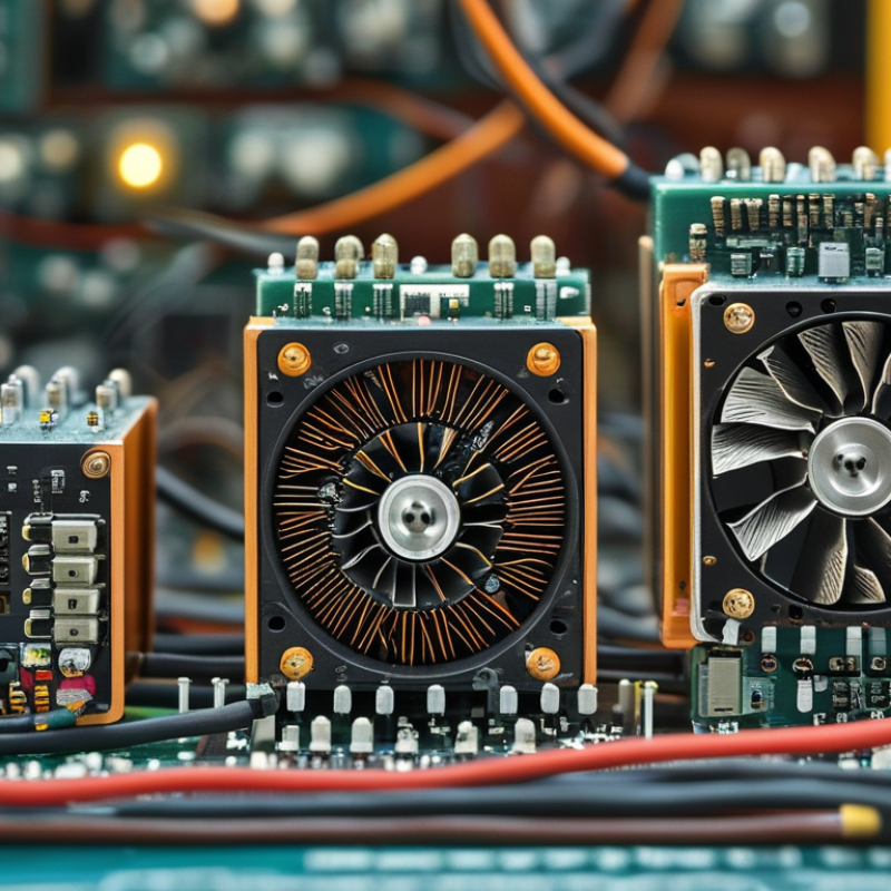
Top Ways to Minimize Energy Loss During Power Conversion

Calculate η = Pout/Pin and set a conversion-efficiency target above 95%

Energy loss during power conversion becomes visible when efficiency is measured, not guessed. Use η = Pout/Pin, with both powers recorded in watts. For example, a converter receiving 120 W and delivering 114 W reaches η = 0.95, or 95%. Measure input voltage and current at the converter terminals. Repeat these measurements on the output side. Small wiring losses can distort the result. They matter.

Set a conversion-efficiency target above 95%, but define the test conditions clearly. Record ambient temperature, load level, switching frequency, and measurement uncertainty. Use calibrated instruments when possible. A unit may exceed 95% at 70% load, then fall sharply near standby or peak load. Watch the heat sink. A warm enclosure indicates lost power, though it is not perfect evidence. Improve airflow, shorten high-current paths, and select lower-loss switching components. Recheck η after every change.

I have found that rushed measurements create false confidence. Sometimes, probe placement matters more than the redesign. Keep raw readings and repeat the test. Report the lowest stable result, not the most flattering number. This approach supports more reliable engineering decisions.

Choose topologies that keep conduction and switching losses below 5%

Keeping conversion losses below 5% starts with topology, not a late efficiency patch. For a 48 V to 12 V, 20 A converter, a synchronous buck can reduce conduction loss significantly. It replaces the freewheeling diode with a controlled switch. That matters at high current.

Choose switches with low resistance and moderate gate charge. Lower resistance cuts heat during conduction. Lower gate charge reduces the energy needed during each transition. However, the best balance depends on switching frequency. Higher frequency shrinks magnetic components but increases switching loss. Measure under load.

A resonant or soft-switching topology may keep switching loss below 1% at suitable operating points. Careful dead-time control remains essential. Excessive dead time creates unwanted diode conduction. Too little can cause cross-conduction and serious heating. I have seen a converter miss its 5% target because its layout added several milliohms of resistance. The schematic looked excellent. The copper did not.

Use short current paths, wide copper planes, and tightly placed bypass capacitors. Check the converter at light load, rated load, and peak temperature. Losses often rise after the enclosure warms by 20°C. A thermal camera can reveal hot terminals or uneven current sharing. Do not trust one efficiency reading. Test voltage, current, temperature, and switching waveforms together, then adjust the topology or operating point when the evidence disagrees.

Top Ways to Minimize Energy Loss During Power Conversion

Choose topologies that keep conduction and switching losses below 5%

Representative loss budgets for a 1 kW isolated DC-DC converter operating from a 400 V input to a 48 V output at approximately 100 kHz. Synchronous rectification, soft switching, interleaving, and optimized magnetic components can reduce both conduction and switching losses. The combined loss target remains below 5% for each topology.

Use SiC or GaN semiconductors to achieve inverter efficiencies near 98–99%

Power conversion loses energy through switching, conduction, heat, and parasitic resistance.

Silicon carbide and gallium nitride semiconductors can reduce these losses significantly. In well-designed inverters, efficiencies near 98–99% are achievable under suitable operating conditions.

SiC devices handle high voltage and temperature with low conduction losses. They suit industrial inverters, solar systems, and high-power motor drives.

GaN devices switch extremely quickly, which can reduce magnetic component size and switching losses.

However, fast switching demands careful gate-drive design, short current paths, and controlled electromagnetic interference. Small layout errors can create voltage spikes and unwanted heating.

Thermal design remains essential. A cooler semiconductor usually operates more reliably.

Engineers should measure efficiency across light, typical, and peak loads rather than relying on one impressive test point. A 99% result at full load may fall noticeably during standby or partial operation.

That detail is easy to miss.

Practical testing should include

  • infrared inspection
  • oscilloscope measurements
  • long-duration load trials

Capacitor quality, cooling airflow, dead-time settings, and firmware control also affect the final result.

SiC and GaN are powerful tools, not automatic solutions. Their higher switching performance can expose weaknesses elsewhere in the circuit.

Even experienced teams sometimes optimize speed too aggressively.

A slower, cleaner waveform may deliver better system efficiency and reliability.

Optimize thermal paths to keep semiconductor junction temperatures below 125°C

Top Ways to Minimize Energy Loss During Power Conversion

Optimize thermal paths to keep semiconductor junction temperatures below 125°C

Efficient power conversion begins with controlling heat, not merely reducing electrical losses. Semiconductor junction temperature should remain below 125°C under realistic operating conditions. Include ambient heat, enclosure restrictions, airflow changes, and temporary overloads in the calculation. A cool laboratory test can hide serious field conditions.

Use short, wide copper paths between the device, thermal pad, and ground plane. Add correctly sized thermal vias beneath exposed pads to move heat into internal copper layers. Keep high-current traces away from heat-sensitive control components. A low-resistance thermal interface also matters, but excessive interface material can increase thermal resistance. Measure its thickness during assembly.

My first layout looked adequate on paper. The measured case temperature stayed low, yet the estimated junction temperature approached the limit. That assumption was wrong. The missing factor was heat trapped beneath the package. Infrared measurements helped locate the hotspot, but they did not directly reveal junction temperature. Combine case measurements with datasheet thermal models and electrical loss calculations.

Provide airflow around inductors, switching devices, and rectifiers. Avoid placing tall components beside the main heat source. If natural convection is insufficient, redesign the heat spreader before increasing fan speed. Monitor temperature during startup, steady operation, and peak load. Add protective derating when margins become narrow. A design that survives testing may still need refinement.

Top Ways to Minimize Energy Loss During Power Conversion - Optimize thermal paths to keep semiconductor junction temperatures below 125°C

Thermal-path optimization reference table for power electronic assemblies
Thermal-path measure Typical material or design Typical thermal conductivity Main design objective Practical implementation guidance
Reduce semiconductor power loss Low-resistance switching device with an appropriate voltage and current rating Application-dependent Lower heat generation at the source Minimize conduction loss, switching loss, and unnecessary gate-drive loss without compromising safe operating area or reliability.
Use a short copper heat-spreading path Copper baseplate, copper heat spreader, or thick copper PCB region Approximately 390–400 W/m·K Spread heat rapidly and reduce local hot spots Keep high-current and high-heat regions compact; use wide, short copper paths and avoid unnecessary thermal bottlenecks.
Select a suitable aluminum heat sink Extruded or machined aluminum heat sink Approximately 200–235 W/m·K Provide sufficient surface area with low mass and cost Orient fins to support natural convection or the intended forced-air direction. Keep airflow passages clear.
Minimize interface resistance Thin thermal interface material, phase-change pad, or thermal grease Material-specific; often about 1–10 W/m·K Remove air gaps between mating surfaces Use the thinnest practical layer, control mounting pressure, and maintain flat, clean contact surfaces. Contact resistance depends strongly on surface finish and pressure.
Improve electrical isolation without blocking heat Aluminum nitride or alumina ceramic insulation layer Aluminum nitride: about 140–180 W/m·K
Alumina: about 20–30 W/m·K
Maintain isolation while limiting thermal resistance Choose the thinnest qualified dielectric layer that meets voltage, creepage, clearance, mechanical, and reliability requirements.
Increase convection effectiveness Natural convection or forced-air cooling Heat-transfer coefficient varies widely Lower heat-sink-to-ambient thermal resistance Provide unobstructed inlet and outlet paths, avoid recirculation, and account for fan performance degradation caused by filters and pressure drop.
Use the enclosure as a heat-spreading surface Metal chassis or thermally connected enclosure wall Aluminum: approximately 200–235 W/m·K Increase external radiating and convecting area Thermally couple the heat source to the enclosure while preserving touch-temperature, insulation, ingress-protection, and mechanical requirements.
Control printed-circuit-board thermal spreading Large copper pours, thermal vias, and multilayer copper planes Copper: approximately 390–400 W/m·K Move heat away from packages and reduce PCB hot spots Use arrays of appropriately sized thermal vias and connect them to internal or backside copper areas where electrical design permits.
Limit thermal bottlenecks in mechanical joints Flat mounting surfaces, controlled fastener torque, and uniform clamping System-dependent Maintain consistent contact over the full heat-transfer area Prevent tilt, bowing, pump-out, and uneven pressure. Validate the assembly after thermal cycling and vibration testing.
Design for a junction-temperature margin Thermal design using junction-to-case, case-to-sink, and sink-to-ambient resistance Target Tj < 125°C Prevent excessive temperature and improve reliability Use worst-case ambient temperature, maximum semiconductor loss, airflow tolerance, interface aging, and manufacturing variation in the calculation.
Core thermal calculation
Tj = Ta + Ploss × (RθJC + RθCS + RθSA)
Where Tj is junction temperature, Ta is ambient temperature, Ploss is semiconductor power loss, and the three resistance terms represent junction-to-case, case-to-sink, and sink-to-ambient thermal resistance.
Illustrative design check
At Ta = 40°C, Ploss = 45 W, and total thermal resistance = 1.6°C/W: Tj = 40 + (45 × 1.6) = 112°C.
This leaves a 13°C margin below a 125°C design limit. Actual results must be verified using measured power loss, validated thermal-resistance data, and worst-case operating conditions.
Material conductivity values are representative room-temperature ranges; actual performance varies with composition, temperature, thickness, surface condition, pressure, orientation, and aging.

Validate efficiency with IEEE 1459 measurements at 25%, 50%, and 100% load

Efficiency claims often look impressive at full load. Real systems rarely operate there. Validate power conversion with IEEE 1459 measurements at 25%, 50%, and 100% load.

At each point, record active power, apparent power, reactive power, and current distortion. Measure input and output simultaneously, using a calibrated power analyzer. A converter may show 96% efficiency at full load, but only 90% at 25%. Fans, control circuits, and standby losses become more visible at light loads. Load steps matter. Allow temperatures to stabilize before recording results.

The 2024 Uptime Institute Global Data Center Survey reported an average PUE of 1.56 for 2023. This figure includes facility overhead, so conversion losses deserve separate inspection. The International Energy Agency estimates data-center electricity demand could exceed 1,000 TWh by 2026. Small efficiency gaps can therefore scale quickly. IEEE 1459 also helps separate useful power from distortion and reactive components, preventing misleading efficiency claims.

A practical test sheet should show every reading, instrument uncertainty, ambient temperature, and load duration. Numbers can disagree. That is useful. Recheck wiring, phase balance, and sensor placement before changing hardware. One weakness remains: three load points may miss a sharp loss peak between 50% and 100%. A finer sweep is better when the application changes rapidly. Anomalies deserve attention, not deletion.

FAQS

: Which topology can reduce losses in a high-current converter?

: A synchronous buck topology can reduce conduction loss by replacing the freewheeling diode with a controlled switch.

How should switching devices be selected?

Choose low-resistance devices with moderate gate charge. Lower resistance reduces heat, while lower gate charge reduces transition energy.

Can higher switching frequency improve efficiency?

Higher frequency can shrink magnetic components, but it also increases switching loss. Measure efficiency under realistic load conditions.

Why is dead-time control important?

Excessive dead time causes unwanted diode conduction. Too little dead time can create cross-conduction and severe heating.

Which layout details help reduce conversion loss?

Use short current paths, wide copper planes, and bypass capacitors close to switching devices.

What operating conditions should be tested?

Test light load, rated load, and peak temperature. Losses may increase after the enclosure warms by 20°C.

How should efficiency measurements be validated?

Measure at 25%, 50%, and 100% load. Record active power, apparent power, reactive power, and current distortion.

Why can light-load efficiency be disappointing?

Fans, control circuits, and standby losses become more visible at light loads. Full-load efficiency is not enough.

What should a reliable test sheet include?

Include every reading, instrument uncertainty, ambient temperature, and load duration. Allow temperatures to stabilize first.

Is testing only three load points sufficient?

Not always. Three points can miss a sharp loss peak between 50% and 100% load. A finer sweep may reveal it.

Conclusion

Minimize Energy Loss During Power Conversion by treating efficiency as a measurable design objective from the beginning. Calculate efficiency using η = Pout/Pin and establish a target above 95% for the complete conversion system. Select circuit topologies that limit combined conduction and switching losses to below 5%, while using advanced wide-bandgap semiconductor materials to support inverter efficiencies of approximately 98–99%. Careful component selection, switching-frequency control, and optimized operating points can further reduce unnecessary power dissipation.

Thermal management is equally important because heat directly affects performance, reliability, and service life. Design short, low-resistance thermal paths and maintain semiconductor junction temperatures below 125°C under expected operating conditions. Finally, validate the results through standardized IEEE 1459 measurements at 25%, 50%, and 100% load. Testing across these conditions reveals partial-load weaknesses, confirms the efficiency target, and ensures that reported performance reflects practical operation rather than a single ideal test point.

Mason

Mason

Mason is a seasoned marketing professional with a deep expertise in the company's offerings and a passion for driving brand awareness. With a strong background in digital marketing strategies, he has an innate ability to connect with diverse audiences and effectively communicate product benefits.......